~ Roll to Roll ~
One of the features of NISSHA’s mass production technology is its roll-to-roll process technology using a roll film as the base material.
The photo-etching process using a large-area photomask of up to 500 mm x 1,000 mm achieves high positional accuracy and high throughput by using excellent roll transport technology.
Introducing NISSHA’s technology for manufacturing thin film devices, from roll-to-roll patterning processes to individual piece cutting and bonding to chassis components.
We have an advantage in mass production using roll film of 500mm width.
We can handle from patterning to individual cutting and module production.
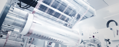
Outstanding roll-to-roll transport technology
NISSHA’s COP film used for touch sensors is a highly transparent optical film comparable to glass. However, COP has a very fragile property, and it is very difficult for thin COP film with a thickness of less than 100μm to pass through the production line. Nissha’s unique equipment development technology has realized the transport of such difficult-to-handle film materials up to 55um in mass production and up to 30um for developed products.
Fine patterning of Line / Space = 10 / 10μm level
NISSHA’s photo etching process enables precise alignment of wiring with a line width of only 10μm on the front and back of the film. Also supports patterning of multi layer of thin metal like ITO + Cu.
Material selection according to the purpose of the device
We have accumulated a wealth of know-how on materials necessary for device manufacturing, such as transparent films, conductive materials, and insulating films.
Modular processing technology that realizes the delivery form according to the customer’s request
Special technology to cut without cracking even fragile films like COP. We will deliver products in the form of processing according to customer requirements, from the patterning of film parts to module parts integrated with housing parts, such as bonding technology for mounting film sensors on large resin molded products.
| Photolithography / etching | Thin metals of Cu, ITO, etc. | L/S = 10/10μm |
|---|---|---|
| Screen printing | Printing of conductive pastes such as Ag, carbon, PEDOT, etc., and insulating films and adhesives |
L/S = 50/50μm |
| Laser etching | L/S = 30/40μm | |
| Post-processing (module processing) | Processing individual modules from rolls Film laminating, punching, FPC bonding, housing bonding |
|
A high level of technical skills is needed to process these devices and process film devices. One of the features of NISSHA’s technology is that it can handle multiple processes consistently as one stop solution.
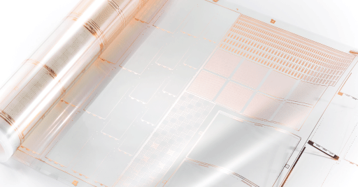
Etching
Patterning of ITO, Cu, Ni, other alloys and insulating films
Screen printing
Printing of conductive pastes such as Ag, carbon, PEDOT, etc., and insulating films and adhesives
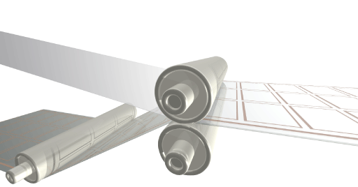
Insulating film
Improve durability
Add functions such as electrical insulation
Optical function film
Lamination of polarizing film, etc
In addition, lamination of film materials
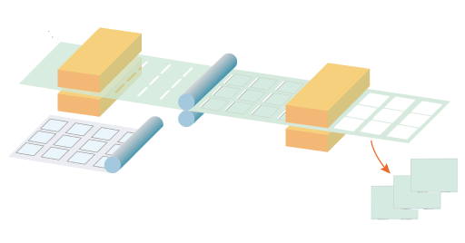
Supports die cutting, laser cutting, and half cutting with high dimensional accuracy
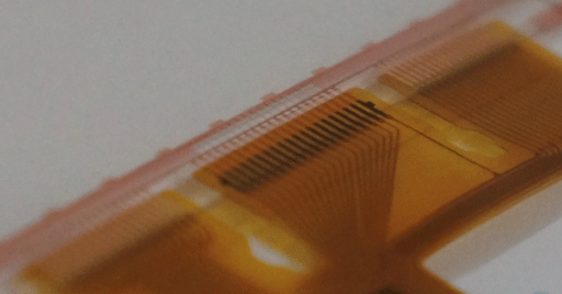
FPC bonding process using anisotropic
conductive adhesive (ACF)
We propose a process suitable for product specifications, such as bonding to double-sided terminals.
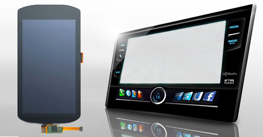
We can provide one-stop housing modules
such as bonding with resin molded products
produced by our IMD technology, bonding of cover glass
and film devices.
In order to provide products that satisfy customers, we have introduced a design review system that establishes a design that satisfies the required specifications at an appropriate cost and enables stable mass production.
1.Check if it can be accepted
Review the technical difficulty of the customer’s required specifications.
While coordinating between the technical department and the sales department, information such as material design, process technology, and cost adequacy will be organized and it will be examined whether it can be entrusted.

2.Organize a project team for each project
If it is confirmed that the contract can be accepted, a project team will be formed for each project.
The team is made up of members selected from each of the technical development, design, production technology, evaluation technology, and quality assurance departments, and plans for mass production.

3.Validate your design with small-lot production prototypes
Verification of design validity through small lot prototypes.
We perform mass production suitability evaluation, failure mode analysis, reliability evaluation, etc., and confirm the optimal mass production conditions.
Prototype results will also be reported to customers, confirming that there is no problem even if they shift to mass production.

4.Mass production to delivery
After preparing the mass production transfer document based on the results of the prototype verification, the project is transferred to the mass production department and mass production is started.

5.Quality control of mass-produced products
After mass production, the quality assurance department manages whether stable production is running or whether there are no defective products outgoing. The quality assurance department joins the project from the design verification stage, enabling intrinsic quality assurance.

Electronic devices are evolving every day. In response, designers have to think and shape products that no one has ever made.
In order to create a unique new product, a device that is not a general-purpose module but is uniquely designed is required.
We, NISSHA, have prepared technologies and equipment to respond to such customer needs.
If you have any difficulties in manufacturing electronic devices, please contact us.
Please feel free to contact us for any questions or consultations on film devices, including consultation on development, trial production, mass production consignment, etc.
CLICK