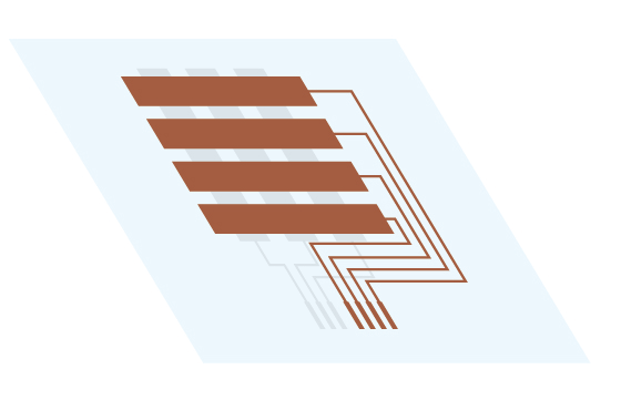
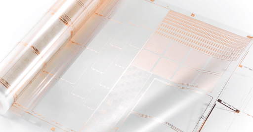
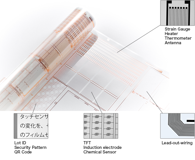
High-definition patterning of thin films of ITO, Cu, Ni, etc.
Electrodes and wiring patterns are processed by a roll-to-roll etching process.
Our strength is that we have two processes, photolithography and screen resist, and can process with high precision
| Film forming material | Various metals such as ITO, Cu, Ni and their alloys |
|---|---|
| Base film | COP (ITO / Cu), PET (ITO, Cu alloy, etc.) |
| Mask size | 500×500㎜ |
| Processing accuracy | Line/Space =10/10µm |
Please consult us about the patterning and post-processing of other materials from the inquiry form.
High-precision wiring processing with Line / Space = 10 / 10µm, double-sided processing, and large area are available.
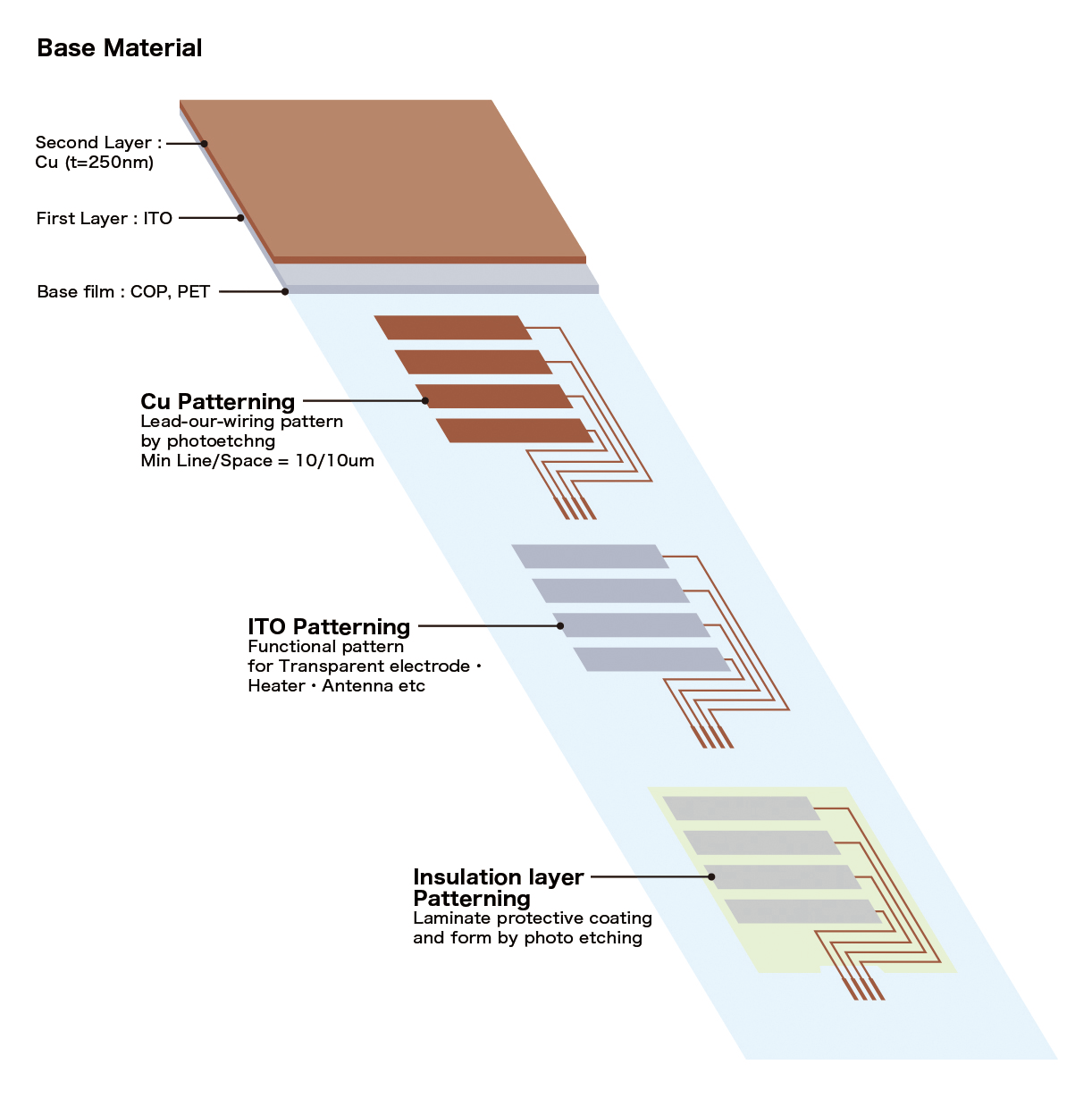
It can be processed on both sides of the film, not just one side. Alignment with an accuracy of 10um or less is achieved.
Supports large area patterning with a mask size of up to 500 x 1,000mm
It responds to a wide range of needs such as multi-cavity for mass production and production of large modules.
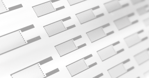
We can also pattern copper alloy thin films used for strain gauges.
Raw material
Cu alloy thin film (t = 100-200nm) / Base film (PET)
mask size 500 × 500㎜
Post-process such as insulation coating processing and individual cutting is also possible.
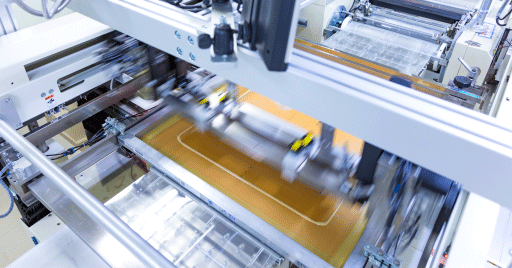
We have a process for resist processing by screen printing.
Since no photomask is required, low-cost production is possible.
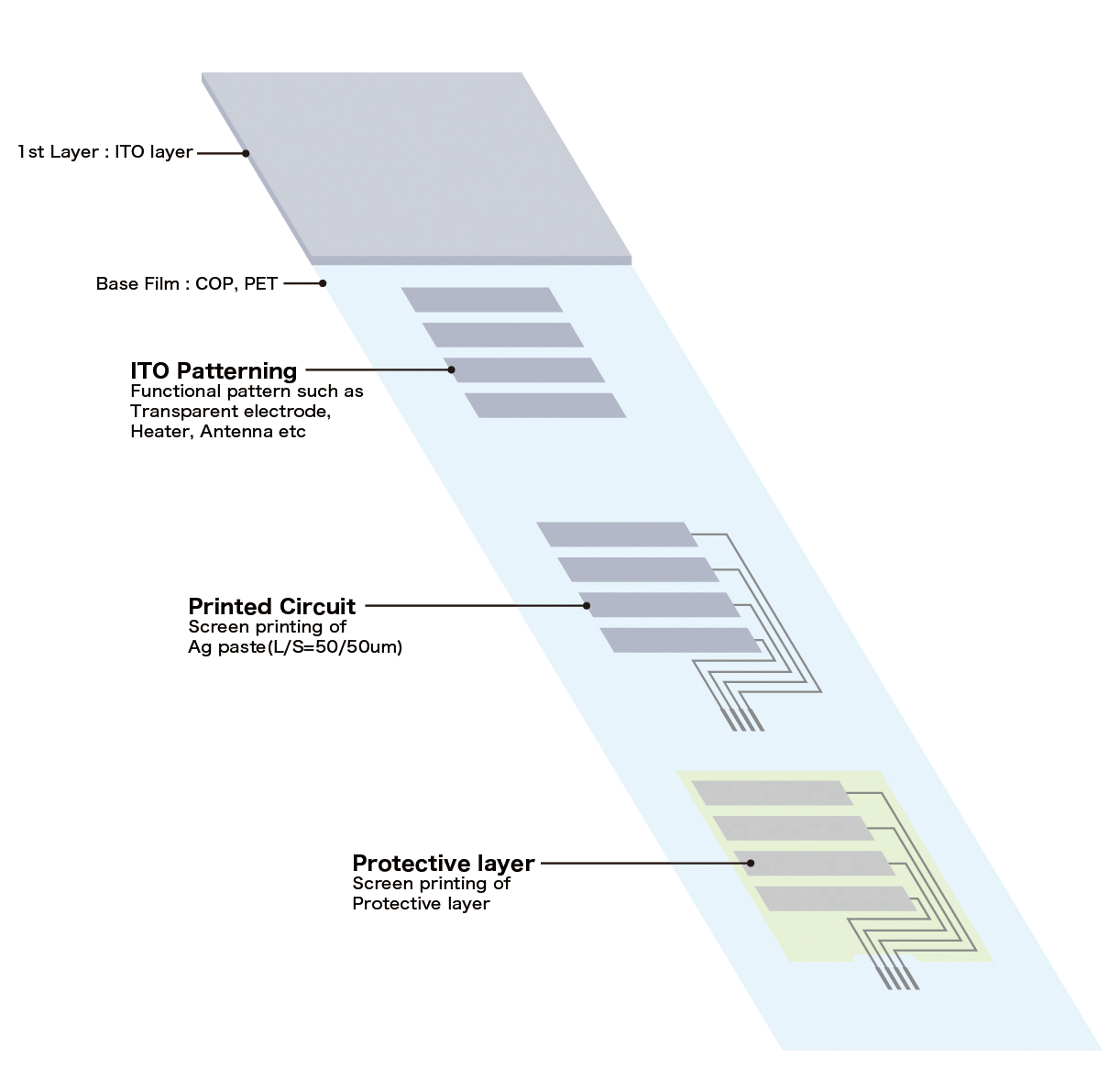
| Film forming material | ITO |
|---|---|
| Base film | PET |
| Screen size | 500×500㎜ |
| Processing accuracy | Line/Space =50/50µm |
Please consult us on the inquiry form for patterning and post-processing of other materials.
Please feel free to contact us for any questions or consultations on film devices, including consultation on development, trial production, mass production consignment, etc.
CLICK