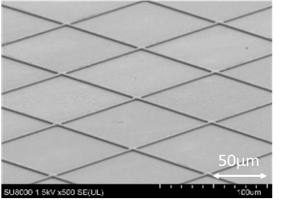
Process development for achieving both lower resistance and narrower line width pattern on transparent film
NISSHA is developing the SAP process.
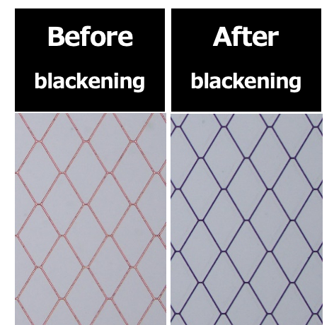
We add high value to the flexible substrates utilizing fine patterning technology.
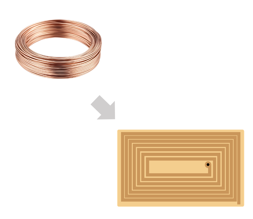
The technology may be applicable to various products such as transparent antennas.
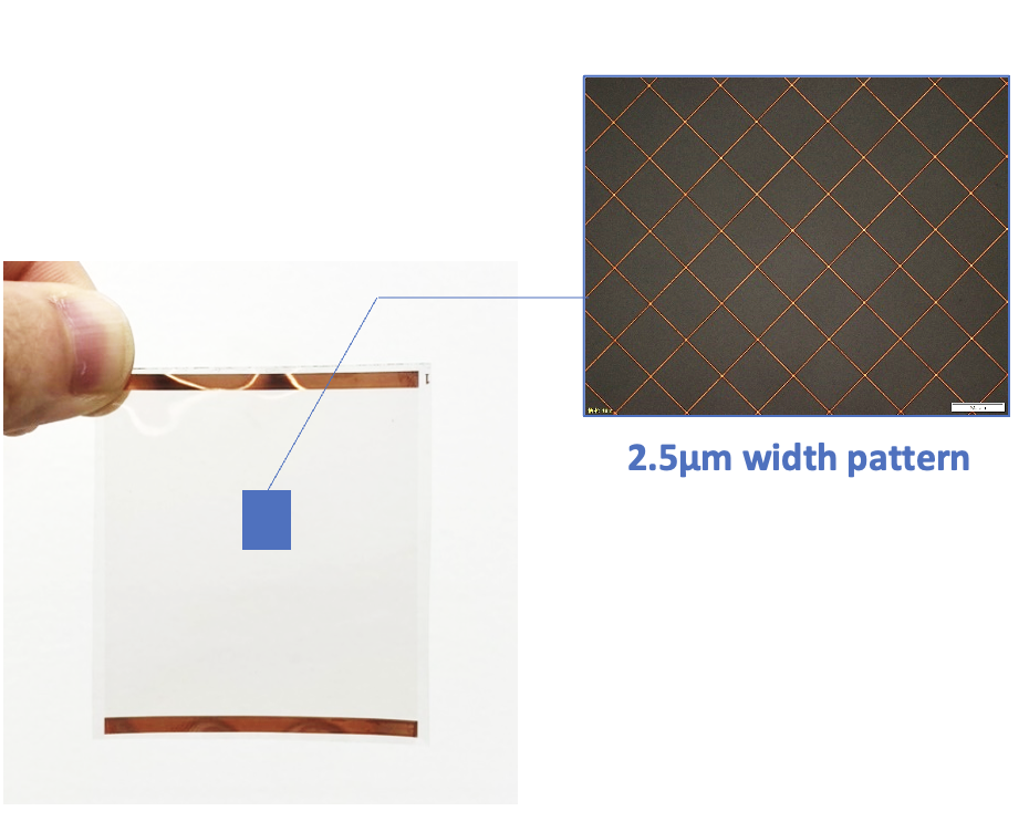
High optical transparency is enabled by fine patterning capability and intrinsic optical properties of substrate material, COP.
Both low electrical resistance and narrow line width are attained due to fine patterning and plating technologies.

Our current manufacturing line consists of both roll-to-roll and sheet-to-sheet processes. We will be launching a fully roll-to-roll line that can process 500mm width webs for mass production.
SAP has the following features compared to subtractive process.
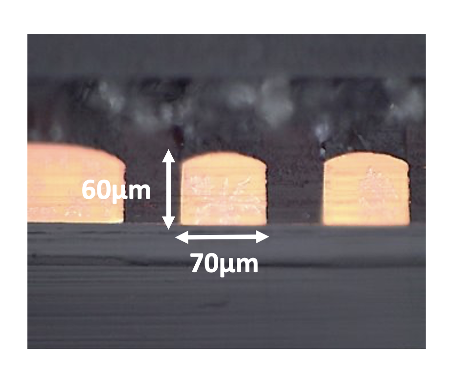
・Narrow traces can be patterned
・Thickness of Cu can be adjusted
・Rectangular cross section of traces
| SAP (under development) |
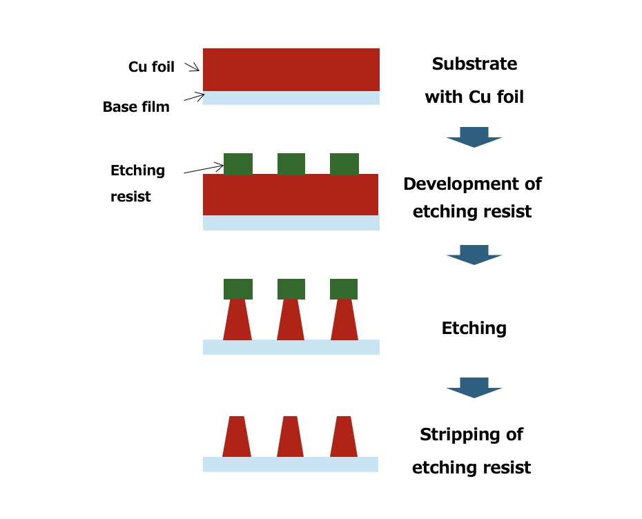
Subtractive process (NISSHA conventional process) |
|
|---|---|---|
| Process flow | 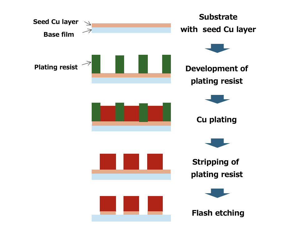 |
 |
| Base film | COP, PET, PI, etc. | COP, PET, PI, etc. |
| Plating material | Cu | Various metals such as ITO, Cu, Ni,etc., and their alloys |
| Mask size | Max 500×600mm | Max 500×600mm |
| Trace width | 5μm * Contact Nissha |
10μm * Contact Nissha |
| Patterning process |
Single-sided *Double-sided patterning is under development |
Single-sided and double-sided |
![]()
![]()
Copper consumption is expected to be reduced for 70% by changing the process from Subtractive to Semi-Additive.
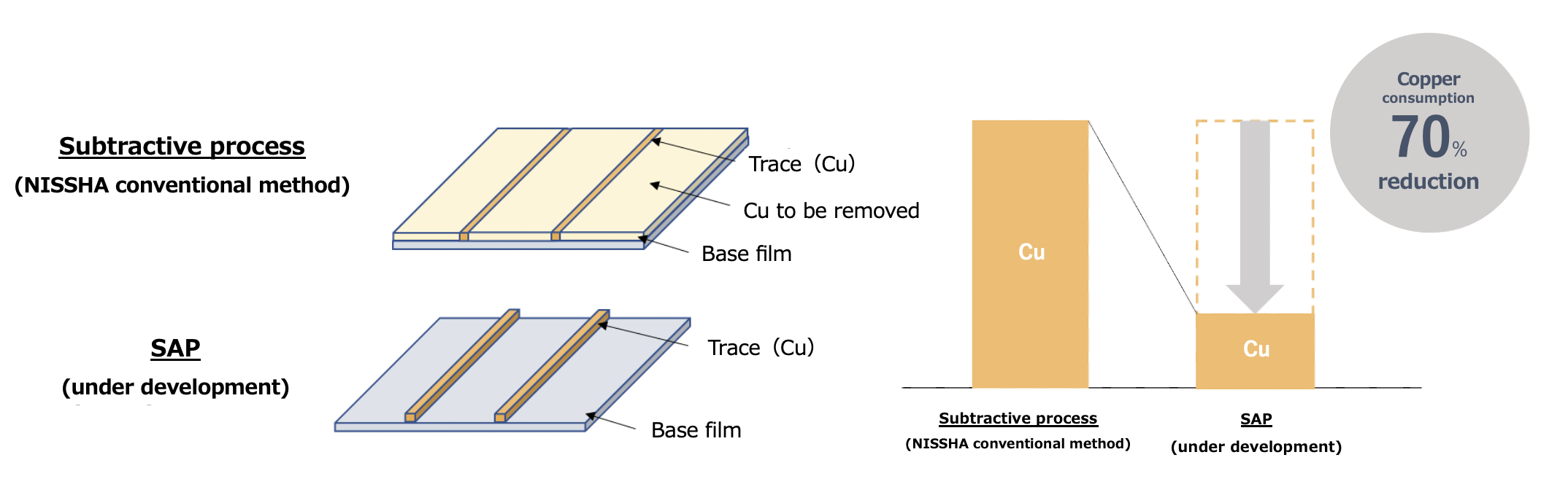
*Estimate conditions
10μm thick Cu, traces cover 30% of the entire surface.
Please feel free to contact us for any questions or concerns.
