We have a wealth of knowledge on pasting, crimping, and patterning of special materials to add various functions required for devices.
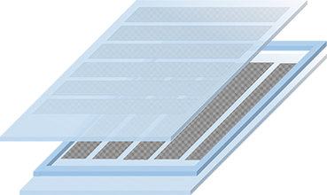
Laminate and pattern a transparent insulating film to protect the wiring pattern. By controlling the refractive index of the transparent insulating film, the high transparency of the ITO pattern is not impaired.
In laminating transparent films, we optimize the transparent adhesive and processing conditions so as not to impair optical properties such as transparency and low refractive index.
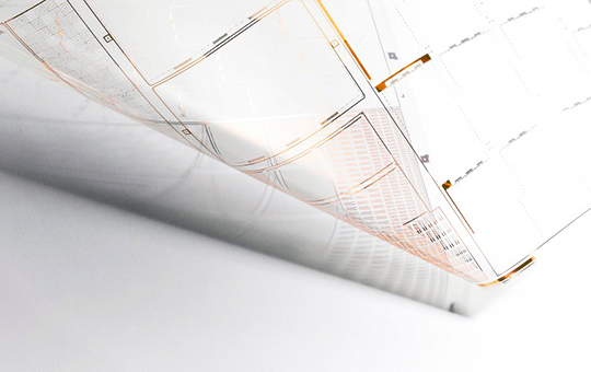
The wiring mask pattern, which was conventionally formed by printing on a glass panel, is formed on the wiring pattern using a photosensitive insulating film. By improving the masking position accuracy, it is possible to design a large transparent area.
It is used for narrowing the frame around the display.

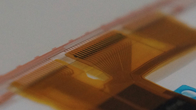
The lead wire and the FPC are bonded using an anisotropic conductive adhesive. Anisotropic conductive adhesive is a material that conducts electricity only in a specific direction. The wiring on the film and the wiring on the FPC are connected one-to-one.

It is a transparent conductive film formed by sputtering an indium tin oxide semiconductor. High transparency with total light transmittance of 90% or more.
Sheet resistance value: 70 to 100Ω /□
Low-resistance conductive material suitable for current collection wiring of semiconductor devices and sensors. Our photo etching process specializes in 100 to 250nm thick Cu thin films.
Volume resistivity 2.5μΩ/cm
Wiring material commonly used in screen printing. Materials are selected according to customer requirements such as resistance value, line width, and flexibility.
A material in which a nano-sized ultrafine fibrous silver filler is filled in a transparent resin. Since the filler cannot be seen, a transparent conductive film is formed. Compared with ITO, it has excellent flexibility and electrical characteristics.
Flexible display, touch panel, solar cell, etc.
Ink used for resistance film type pressure sensor. The printing surface forms a fine rough surface.
The pressure is detected from the change in resistance that occurs according to the change in the contact area of the upper and lower electrodes due to pressing.

It is a very transparent film material with excellent optical properties. There is no rainbow reflection due to light refraction.
Displays, windows, optical analyzers, etc.
A transparent material used as a general-purpose base film. Excellent heat resistance, break resistance, chemical resistance, etc.
We will select materials according to customer requirements, such as PC, PEN and PI.
We support your consideration through various communications.
– We will contact you quickly by e-mail, telephone, Skype.
– We will prepare samples and data according to the contents and visit.
* Please note that it may not be possible to respond depending on conditions such as remote locations.

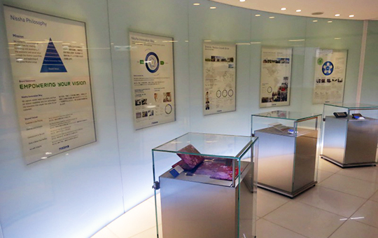
The Nissha Gallery at the Kyoto headquarters offers a wide range of products.
Please feel free to apply for a tour.
* We do not open to the public.

Please feel free to contact us for any questions or consultations on film devices, including consultation on development, trial production, mass production consignment, etc.
CLICK